
Research in the deep freeze: Fraunhofer IZM develops integration techniques for cryo-electronics
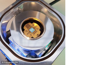
It is a common trope in science fiction: The novel’s or film’s protagonist is put into stasis in a cryochamber, only to wake up hale and sound even though centuries have passed in the meantime. As far-fetched as this might seem, the idea is grounded in real-life science: Cryotechnology. It works by turning gasses into liquids at temperatures of below -160°C. Long a reserve of experimental research since the principles of cryotechnology were developed in the late 19th century, the technology has recently attracted the attention of many people in industry for the great practical potential of working at such extreme temperatures: In spaceflight, cryosensors are used for gravitational measures or for low-noise amplifiers for extremely weak signals in the vastness of space. Cryosurgery can help treat damaged tissue. But one field where cryotechnology really comes into its own is: Quantum technology. The quantum world holds much promise in many practical fields, from computing or sensor technology to quantum communication. But this promise will only come true once working and, above all, genuinely scalable production technologies are available. For a quantum computer to run calculations and accelerate actual applications, it needs additional qubits that it can work with – hundreds of thousands or even millions of tiny physical bodies. These qubits are connected with each other via superconducting circuits, which have hardly any measurable electrical resistance once they are cooled down past a certain threshold. But reading and manipulating qubits needs an electronic switch with sufficient port density, and it needs to be thermally decoupled to stop its own heat signal from destroying the quantum entanglement of the qubits. What theorists call quantum supremacy – the point at which quantum computers outperform the most powerful conventional computers – can only be achieved with high numbers of qubits. Researchers expect this number to range in the six or seven figures, but the actual number of qubits that could be placed on a semiconductor chip is generally limited by the port density. Current technology has been stuck at a pitch, i.e. the distance between individual contacts, of 15 micrometres for several years, but now the research team of Dr Hermann Oppermann of the Fraunhofer Institute for Reliability and Microintegration IZM has achieved the seemingly impossible: With galvanic deposition of indium, they created a pitch of less than 7.5 micrometres.
As the system needs to be kept at a temperature of 20 milli-Kelvin during operation, its electrical connections can only give off minute amounts of thermal energy. This is what superconducting materials were created for. Hermann Oppermann and his fellow researchers managed to deposit and structure superconducting niobium and niobium alloys, the materials used for contacting vias through several layers of substrates, in socalled interposers. The end product of their work is an extremely low-loss circuit carrier that can connect entire qubit arrays in real time and integrate them into highly dense, but scalable systems for quantum computing.
Fraunhofer IZM set up a dedicated cryometric lab in Berlin as the place where this fundamental technology could be developed, suitable materials tested, integration concepts optimized, and superconducting interconnect technologies trialled for cryogenic applications. The new lab facilities let the researchers test, characterize, and evaluate electrical circuits and make progress with integration technologies for extremely low temperature scenarios. Individual circuit components are cooled down to an unimaginable 3 Kelvin to analyse their resistance properties and draw conclusions about their electrical performance and the reliability of the vias, redistribution layers, and control systems at cryo-temperatures.
Projects are under way to explore new packaging and interconnection technologies for integration under cryogenic conditions, and first measurements have already produced results. “As one of our next steps, we will be moving this cryogenic packaging and interconnection technology in the direction of high-frequency, millimetre-wave technology.” Hermann Oppermann has reasons to be optimistic: “We are constantly learning more in this field, which is creating amazing potential in the market for possible applications. This is not limited to quantum technology, but also opens up new prospects for conventional applications, like high-performance computing or cryosensors. We are always interested in other projects that could benefit from our expertise with packaging technologies for cryogenic applications.”